TAs, and Office Hours:
- Peter Popplewell: Thurs 11:30-12:30, ME 5138
(Blue Room)
- Tony Forzley: Lab weeks: Wednesday 11:30-12:30,
non lab weeks, wednesday 9:00-10:00, room ME 5137, this is a
room inside of Room 5138
Marks updated Dec 7, 2006. There may still be a few marks
not updated. Let me know of errors, ommissions, concerns, etc.
Exam Review Office Hours for Prof. Plett
- Tuesday Dec 5, 12:30-2:30
- Wednesday Dec 6, 12:30-2:30
Office Hours for Prof. Plett
- Monday 12:30
- Tuesday 2:30
(
right after 4505 class, so I will typically be a bit late
back to my office )
Friday 12:30 (last Friday office hour is Friday Dec 1)
(I meet with fourth-year project students Fri 11:30, so if I am
not in my office, look for me one floor down, probably in one of the
computer labs.)
Final Exam, 2:00 PM Thursday December 7, 2006, in the Fieldhouse
Recent Questions related to studying for final exam
Questions, Answers from 2005
Questions/Answers from 2004.
Questions/Answers from 2003
Assignment 3 Info
Assignment 3 has been marked and can be
picked up Monday afternoon during my consulting hour starting
at 12:30.
Due 1:00 in class Thursday, Nov 30 (our last class)
Since Nov 22, 23, 24 would normally be lab days, we will try
to have a TA available from about 9:30 or 10AM in the computer
room across from the lab (later changed to ME 4128)
on each of those days (Peter on Thursday, Tony
on Friday).
So, if you want to take advantage of this lab time slot, and
do your oscillator SPICE assignment, or have any other questions
for the TAs, you can take advantage of this opportunity.
For Assignment 3, as handed out in class, you will need to copy
and modify the following two programs for oscillator analysis.
Your aim will be to achieve a particular output frequency and
power, and being approximately impedance matched. So, what you
will need to change:
-
Frequency determining components: C1, C2 (LT is given)
-
Load Resistance: RL
-
Resistor to represent transistor output resistance: RE4
(For open loop only)
-
Open loop: Frequency Range in .AC command to center on your frequency,
optimize curves
- Closed Loop: Time range in .TRANS command to show rise time,
maybe zoom in to show a few periods to allow frequency to be
calculated. Make sure where you zoom in, the output voltage
is completely settled.
Assignment 3 Example SPICE file for Open-Loop Oscillator test.
Assignment 3 Example SPICE file for Closed-Loop Oscillator test.
Lab 3 Info
Lab 3 Due date is Tuesday November 21 at 1:00 in class.
Lab 3 Tentative, Approximate Marking
Scheme, probably close to the final value but subject to small
changes. (pdf)
Assignment 2 Info
Assignment 2 Due Dates:
- Questions 1, 2, 3 are due on Tuesday November 7 at 1:00 in
class. Remember, this is also design for Lab 3b, so keep a copy
of this part of the assignment.
- Questions 4, 5, 6 are due on Tuesday November 14, at 1:00
in class.
Assignment 2 (pdf)
Lab 2 Info
For all sections, Lab 2 is now due on Tuesday Oct 24 1:00
in class at the beginning of the class.
Extra Notes for Lab 2 - written by
Tony who will be marking this lab. (PDF)
Lab 2 Marking Scheme (PDF)
This may not be quite final yet, but it should give you an idea
of what is being looked for.
Inductor Q at 100 kHz and 1.2 MHz.
From results, we suggest you use the 33 uH inductor to get the
highest parallel resistance. In the lab you can measure Q at
100 kHz, then estimate Q at 800 kHz by assuming Q is proportional
to the square root of frequency.
(The final filter gain calculation equation has
been modified so gain is inversely proportional not proportional
to (fu-fl)/(Bw/2)
SPICE File For mixer
This is not required for the lab, but you may find it interesting
and useful. Note, this is a nonlinear circuit, so simulations
are in the time domain. Tos see output spectrum including harmonics
and intermodulation components, run the fft on the output transient
waveform. Note that for this simulation, discrete 2N3904 transistors
have been used, but in spite of this, the results are quite realistic.
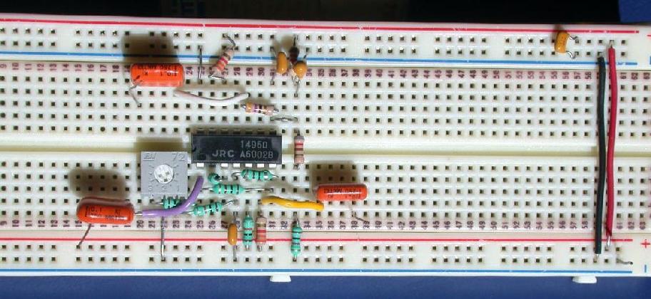
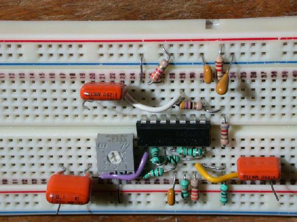
Photo of a Neatly Constructed
Mixer Board. Note that pin 7 has been used as an interconnect
point. It is labelled on the diagram as NC for No Connect. Often
it is not a good idea to use such pins, but in this case it seems
to work. (I still wouldn't do it though.) Also, note the yellow
wire hides a connection. Don't believe it?
Check out this picture from a different angle.
Lab 2, Mixer: Important Points:
-
Bring your breadboard, wire strippers, and mini screwdriver for
construction of circuit.
-
Bring a floppy to store measurement results from scope.
-
Do construction ahead of time, if possible to save about one
hour of lab time.
Assignment 1 Info
Assignment 1 Example.
Very speedily dashed off example solution to Assignment
1, but done for centre frequency of 1 MHz, bandwidth of 325 kHz,
following the lab 1 info posted earlier. If you find errors in
this, let me know.
-
You may choose to use Zin either from your calculations, or from
the simulation. These are known to be quite different because the
value stated for Cbe (Cpi) in the lab manual is quite a bit off
(it is listed as being 8 pF, but if you examine your SPICE output
file you will see a value more like 30 pF is used in the simulation).
Lab 1 Info
** Date Corrected ** For all sections,
Lab 1 and Assignment 1 is now due on Tuesday Oct 10 (after Thanksgiving),
1:00 in class at the beginning of the class.
Lab preparation is important, otherwise, this can be a long lab.
Lab 1 Held in Computer Room, next to hardware lab, ME4166
Lab 1 Approximate Marking Scheme 2005,
(PDF)
(similar to 2006, except specs are different, e.g., frequency,
bandwidth etc.)
SPICE File For Lab 1.
Lab 1 Information, somewhat edited Sept 23, 2006.
Lab 1 Information, Improved, with Pictures, Sept
26, 2006, updated 6:00 PM. Note: Comment about RL
has been changed - RL should not be replaced by Rp, rather Rp
should be included in it, both RL and RP should be taken into
account. The net small-signal resistance R (which is determined
by RL, Rp and ro in parallel) sets the overall loop bandwidth
- that is 1/(RC) is the bandwidth. Rp is determined by the Q
of the inductor (not the Q of the overall circuit).
PSPICE Student Version, exe file (28M) Note, this exe file
will unpack a few files. By default, it unpacks them in some
strange location, hard to find, so it is suggested you change
it to a known directory. Then you need to run the setup.exe file.
Click
here to request or download the 683MB OrCAD 15.7 Demo CD which
contains PSpice A/D. Direct from OrCAD
Note: the 28M version in the previous link is an older version of
PSPICE, but it will still do the job)
Link to the year 2005.
Link to the year 2004.
Link to the year 2003.
Course Objective
To learn about the design of
communications circuits. In other courses, the block diagram
approach has been used but in this course the emphasis will be
on the actual circuitry which makes up these blocks. Examples
of such blocks are tuned amplifiers, mixers, oscillators, phase
shifters and detectors. Communications systems considered are
AM, FM, television and telephony. Use of the PLL will be discussed.
Course Content
- Introduction to Telecommunications:
Components of a radio systems; noise, distortion impedance matching.
- Mixers and Modulators:
- Phase-Locked Loop and Applications:
Introduction to PLLs and applications such as:
synthesizers and FM demodulation.
- Oscillators:
- Frequency modulators and demodulators:
- Television Systems:
Transmission of intensity, color, retrace, blanking, and sound;
generation of the video signal, conversion of the video signal
to picture and sound. Other topics may include high-definition
TV, stereo sound.
Labs
Simulation Labs - Groups of 1; Hardware Labs - Groups of 2, one
writeup per group, due one week after the scheduled lab day, 4:30 PM.
- Tuned Amplifiers: (Dates tentative)
(Warmup on September 15, 16, 17 actual lab on 29, 30, October
1). Simulation Lab. Use of a bipolar transistor and some passive
components to build a tuned amplifier operating at about 1MHz.
You will learn about use of transistor parameters, tuned circuits
and impedance matching.
- Mixers and Modulators:
(October 13, 14, 15) Use of an analog multiplier on an IC to
build frequency changers.
- Phase-Locked Loops:
(October 27, 28, 29 and November 10, 11, 12) Use of a commercially
available package to build a tracking filter, a synthesizer and
a an FM demodulator. The IC contains a voltage-controlled oscillator
a phase detector, and amplifiers. In this lab, the VCO and phase
detector will be characterized, then a complete phased-lock loop
will be built. The main external components will consist of a
simple loop filter and a divider to realize the synthesizer.
Marks:
a) Three assignments worth 5% each
b) Three Labs worth 10, 10,15 (about 1/3 for demo)
c) One written exam worth 50%.
**** Students must get at least 35% in the final exam. ****
Text:
There is no official course text. The printed course notes should
provide enough material, or some of the references can be consulted.
References:
- Smith,
"Modern Communication Circuits", Second Edition McGraw-Hill 1998, TK6553.S5595
- Krauss, Bostonian, Raab,
"Solid State Radio Engineering", Wiley 1980, TK6553.K73
- Rogers and Plett,
"Radio Frequency Integrated Circuit Design", Artech House 2003
- Hagen,
"Radio Frequency Circuit Design", Cambridge Press, 1997
- William F. Egan,
"Frequency Synthesis by Phase Lock", 2nd Ed. John Wiley & Sons,
2000
- Van der Puije,
"Telecommunication Circuit Design", Wiley 1992, TK5103.V
- Sinnema, McPherson,
"Electronic Communications", Prentice-Hall 1991, TK5101.S537
- Sedra, Smith,
(for intro to tuned amplifiers, oscillators)
- Stremler,
"Introduction to Communication Systems", (or other intro texts)
- Signetics,
"Linear Data Manual Volume 1: Communications", 1987
For Prof and TAs only: Password Required (board)
Password Required (Lab)
Password Required (L3A_s)